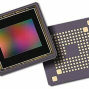
| ON Semiconductor has expanded its high-performance XGS family of Global Shutter CMOS image sensors with two new models; the XGS 9400 and the XGS 8000. These devices provide resolutions of 9.4 and 8.8 Megapixels respectively in a compact package, achieving high-speed performance in a single form factor. Both models contain a rich feature set and are particularly suited for integration into 29 x 29 mm2-cameras for Machine Vision, ITS, Security, Medical and Scientific applications.
The XGS family is available with different resolutions in a single package, all image sensors are pin-compatible. The XGS 9400 is a 1/1.2″-type square format imager with a 13.9 diagonal and 3.072 x 3.072 active pixels. The XGS 8000 has an optical format of 1/1.1″ and reaches 4K UHDR resolution with a 14.8 diagonal and 4.096 x 2.160 pixels. Both XGS models have a pixel size of 3.2µm and are available in monochrome and Bayer color formats from ON Semiconductor’s long-term value-added distributor FRAMOS®. The imager’s frame rate in high-speed mode achieves a maximum of 128 frames per second (fps) at 12bits over 24 lanes in the 8MP version, and 90 fps in the 9.4MP version. The frame rates of both models can be reduced to 80 fps or 56 fps in low-speed mode by companding the bandwidth and implementing only 12 lanes version. The high speed, 12−bit output can maximally leverage interfaces like USB 3.2, Thunderbolt 2, and 10 GigE for industrial environments. |