The late twentieth to early twenty-first century is known as the silicon age, and the impact of silicon on the electronics industry is almost too large to quantify. But, silicon electronics are close to their physical limits in terms of efficiency and performance. Research initiative the Graphene Flagship is working on the solution — nanomaterials like graphene and graphene related materials (GRMS). In this article, Sanna Arpiainen, deputy division leader for the 2D Experimental Pilot Line (2D-EPL), explains how layered materials will unveil a new generation of electronics, promising new functionalities and applications.
Wonder material graphene is a single carbon atom thick and can therefore be classed as a nanomaterial — a material with at least one external dimension measuring less than 100nm. Despite a small size, nanomaterials promise a whole world of potential for the future of electronics, creating faster, smaller and more powerful devices.
It is thanks to their physical properties that nanomaterials like graphene hold such promise for the electronics industry. Using their unique characteristics, nanomaterials can result in smaller, more lightweight electronics that use fewer resources to build and improve the accuracy of circuit construction down to an atomic level. Nanomaterials have the potential to stretch the boundaries of what we currently think electronics should do or be.
But the properties of each nanomaterial differ, so what about graphene, specifically?
Hot properties
Graphene is the strongest known material, harder than diamond and lighter than aluminium. Most importantly for electronics applications though, graphene is incredible conductive —13 times more so than copper. It is also mechanically flexible, chemically stable and disperses heat.
Electronics applications include detectors, modulators, imagers, sensors and transceivers — all have which have been investigated by the research institutions and partner companies within the Graphene Flagship.
Graphene can also be used for photonic and optical electronic devices. Graphene absorbs a broad range of optical wavelengths — from ultraviolet to the far infrared — enabling ultra-broadband communications way beyond the capabilities of 5G. Plus, when used in optical devices, graphene transforms almost all the light it receives into electric signals. This characteristic results in devices that consume less power and work more efficiently.
Graphene will also play a role in the rise of wearable, flexible electronics. The nanomaterial’s extreme thinness, strength and elasticity make it ideal for this kind of device.
The Graphene Flagship Flexible Electronics Work Package, a research and innovation group within the flagship project, is currently working on conductive textiles, stretchable electronics for smart patches, and electronics for paper-based, disposable smart products — like smart packaging — all using graphene and other layered materials.
Graphene on the market
So, electronics using nanomaterials, including graphene, sound great in theory, but when will they reach the market? The Graphene Flagship aims to bring graphene out of academic laboratories and into society within ten years. To this end, it has already developed numerous successful technologies — over 90 products and 15 spin off companies emerging since the Flagship’s inception in 2013, and each year these numbers grow.
However, to reach the market, many electronics applications rely on the wafer scale integration of graphene on a commercial level. In the next five years, products that don’t rely on wafer scale integration, such as flexible sensors and smart packaging, are expected to appear on the market. For those that do, pilot production is expected in 2025 in the earliest. The 2D Experimental Pilot Line (EPL) has been created to speed up this process.
A foundry for the future
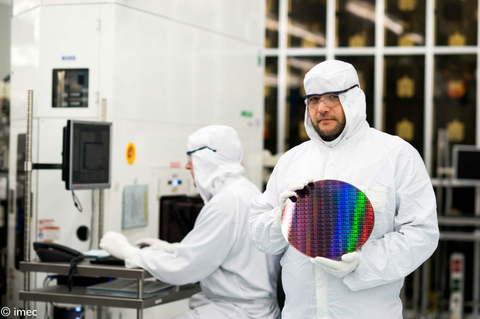
At the start of 2021, the European Commission launched the 2D-EPL, a new €20 million collaborative project to pioneer the fabrication of new electronics, photonic devices and sensors that integrate graphene and layered materials. The 2D-EPL is a graphene foundry, or factory, that offers comprehensive prototyping services to companies, research centres and academics, so they can develop and test their innovative technologies based on 2D materials.
The ultimate goal of the 2D-EPL is to industrialize the production of innovative graphene and layered material-based devices that are integrated with traditional semiconductors. In addition to providing the low and medium volume processing services to advance the component production and integration, the 2D-EPL develops automated high-volume tools and tailored process chemicals compatible with semiconductor industry standards. It will be the first graphene foundry in the world to do so. The 2D-EPL will keep Europe at the forefront of technological innovation, while helping to create the next generation of electronics and semiconductors.
Though silicon has shaped the twenty-first century electronics industry — and in fact wider society too — so far, combining it with graphene and other layered or nanomaterials will push the capabilities of electronic devices much further. A lack of infrastructure has made integrating layered materials with silicon on a large scale a challenge. But, thanks to the 2D-EPL this will change, commercialising graphene and layered material-based electronic technologies.
For more information on the role of nanomaterial graphene in electronics or the 2D-EPL, go to www.graphene-flagship.eu.