
micrometal Group has today detailed some design considertiona which will ensure that when companies migrate away from traditional metal manufacturing processes to photo-chemical etching (PCE) outcomes are optimised and the true power of this next-generation technology is fully realised.
Design engineers are increasingly turning to PCE as they are under pressure to create smaller and increasingly complex precision metal components. As with any process selection, designers need to be aware of the specific aspects of the chosen manufacturing technology when looking at design attributes and parameters. The versatility of PCE and its unique advantages as a precision sheet metal machining technology makes it an engine for design innovation, and can truly be used to manufacture parts that would be deemed impossible if using alternative metalworking technologies.
Jochen Kern, Head of Sales & Marketing at micrometal Group says, “Whether using reel-to-reel or sheet PCE processes, PCE has many attributes that can truly stimulate innovation and ’stretch the boundaries’ with the inclusion of challenging product features, enhancements, complexity, and efficiency. It is vital that design engineers fully exploit its potential, and micrometal advocates that its customers view it as a product development partner — not just a sub-contract manufacturer — early in the design stage allowing OEMs to optimise the potentials that this versatile metal machining process can offer.”
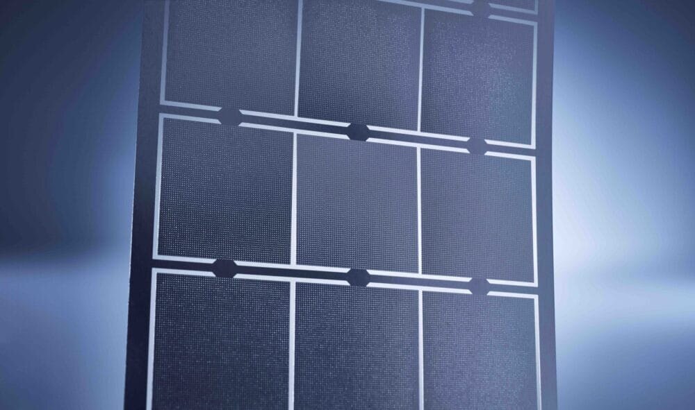
Tolerances are a key consideration in any design and with PCE vary dependent on the material thickness, the material itself, and the skill and experience of the PCE supplier. micrometal Group’s reel-to-reel process is able to produce intricate parts with tolerances as low as ± 7 microns depending upon material and its thickness, this tolerance attainment being unique among all alternative metal fabrication technologies. The company uses a liquid resist system to obtain ultra-thin (2-8 micron) photoresist layers enabling a higher degree of precision in the chemical etching process. It allows micrometal Group to achieve extremely small feature sizes of 25 microns, a minimum hole diameter 80% of the material thickness, and single digit micron tolerances repeatably.

Micro apertures
Kern continues, “As a guide, micrometal Group can process stainless steel, nickel, and copper alloys up to 400 micron thick with feature sizes down to 80% of material thickness and tolerances of ± 10% of thickness. Stainless steel, nickel, and copper above 400 micron thickness, and other materials such as tin, aluminium, silver, gold, molybdenum and titanium can have feature sizes down to 120% of material thickness with tolerances of ± 10% of thickness. Traditional PCE is only able to achieve 100 micron feature sizes and a minimum hole diameter of 100-200% material thickness.”
When it comes to the ability to replicate the exacting accuracy and minimum feature size capabilities of PCE, stamping probably gets the closest, but the trade-off is the stress that is imparted in the metal when it is processed and the residual burrs that are a characteristic of press-working. Stamped parts need costly post-processing, and as expensive steel tooling is used to produce the parts, it is not viable for short runs. In addition, when processing hard metals, tool wear is an issue, with expensive and time-consuming refurbishment often necessary. Many flexure spring designers and designers of intricate metal components specify PCE due to its burr- and stress-free nature, zero tool wear and speed of supply.
Kern comments, “Unique characteristics can be designed into products manufactured using PCE due to the inherent edge “cusp” during the process. By controlling etch cusp a range of profiles can be introduced allowing the manufacture of sharp cutting edges, such as those used in medical blades, or conical openings, such as those used to direct fluid flow in filtration meshes. For OEMs across all industry sectors looking for feature rich, complex and precise metal parts and components, PCE is now the technology of choice as it not only copes well with difficult geometries, it also allows design engineers enormous flexibility, facilitating the adjustment of designs right up to the point of manufacture.”
One major factor that allows for this is the use of digital or glass tooling, which is inexpensive to produce, and therefore inexpensive to change even up to a few minutes before manufacturing commences. Unlike stamping, the cost of digital tooling does not increase with part complexity, which stimulates innovation, as designers focus on optimised part functionality rather than cost. As PCE does not use hard tools, distortion and stress are eliminated. Also, components produced are absolutely flat, with a clean surface and no burrs as the metal is dissolved away uniformly and evenly until the desired geometries are achieved.


")