

Smart systems don’t begin with software. They begin with sensors and actuators, and those, (increasingly) begin with etched metal.
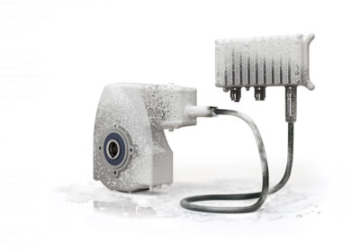
As industries race toward electrification, automation, and ubiquitous sensing, a quiet revolution is happening in the smallest components that make “smart” possible, ultra-precise diaphragms, flexures, springs, meshes, apertures, and shielding elements that convert physical reality into data and motion.
Photo-chemical etching (PCE) is rapidly becoming a preferred manufacturing route for these parts, because it delivers geometric freedom and repeatable precision without the distortions of conventional fabrication.
Unlike stamping, machining, or laser cutting, PCE removes metal chemically rather than mechanically. That means no burrs, no cutting forces, and no heat-affected zones (critical for thin metal geometries that must behave predictably under cyclic loading, vibration, temperature shifts, or exposure to fluids). For sensor and actuator designers, this capability unlocks more than manufacturability, it unlocks performance. Fine features remain true, surfaces stay clean, and elastic behaviour is not compromised by hidden stress.
“Smart systems live or die on repeatability,” says Jochen Kern, Head of Sales & Marketing at the Micro Component Group. “If a spring constant drifts, if an aperture changes effective area, if a flexure picks up distortion, then your calibration, your signal integrity, and your reliability are all at risk. PCE gives engineers a stable way to manufacture delicate, high-function metal features at scale.”
The opportunity is especially relevant today because sensors and actuators are proliferating everywhere, such as in medical wearables and diagnostic platforms, in automotive ADAS and battery management systems, in industrial automation, and in high-frequency telecom hardware.
These applications increasingly demand components that are thinner, lighter, and more integrated, often with multi-functional geometries such as micro-channels, patterned surfaces, or high-density perforations. PCE supports such designs cost-effectively because complexity is largely digital. Phototools can be modified quickly, enabling rapid iteration without hard-tool rework, and proven designs can then transition into high-volume production.
“Many manufacturers are still trying to force modern designs through legacy processes,” Kern adds. “Our role is to remove that friction, helping customers turn ‘too thin’, ‘too complex’, or ‘too sensitive’ into a robust, repeatable part that can be industrialised.”
Manufacturers developing next-generation sensors and actuators are invited to engage with the Micro Component Group to explore how application-led PCE can accelerate design cycles, reduce risk at scale, and unlock new performance possibilities in the components that make smart systems work.


")