Joe Salemi & Mike Albrecht, ZYGO, Middlefield, CT, USA
Silicon Carbide (SiC) optics are becoming more and more prevalent in High Energy Laser (HEL) designs, so it is important that manufacturers are aware of the potential risks when using these materials early in the product development process, thereby avoiding what could be costly and time-consuming problems if discovered too late. Exactly what is possible, and what solutions (and traps) are out there?
The key to success in SiC optics development is to be well informed when it comes to partner selection and material selection, as this will help mitigate program risks especially early on in the design phase.
First of all, it needs to be understood that while price competitiveness is a factor, when looking at SiC for HEL applications, selecting the lowest bidder can often prove more costly in the long run. The chosen product development partner needs to keep an eye on the price for sure, but should also have a high level of market intelligence, material expertise, optics manufacturing expertise, and be an adept engineering consultant.
This is vital as SiC is not a standard “buy, grind, and polish” material. There are many nuances when designing and manufacturing an SiC optic, so the sooner customers access expert feedback from an experienced optical manufacturer, the lower the risk to their programmes. The chosen optics partner should employ a multi-faceted approach ensuring that design, fabrication, coding, and metrology issues are all navigated successfully.
WHY CHOOSE SILICON CARBIDE?
SiC excels in HEL applications, space-based telescope applications, and applications in high acceleration and thermally variable environments.
This is because it exhibits high specific stiffness with a low coefficient of thermal expansion (CTE), excellent thermal stability (desirable so that heat absorption does not affect the beam path), resonant frequency advantages over materials like Zerodur (a key attribute for HEL applications undergoing acceleration), and it can be formed into complex shapes.
It is also non-toxic unlike a key material with similar attributes — beryllium.
THE ANATOMY OF A SILICON CARBIDE OPTIC
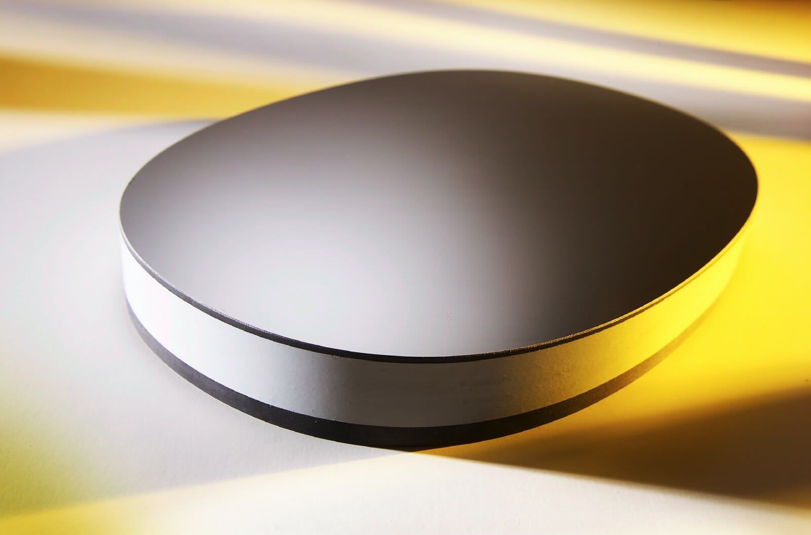
The mirror face of the SiC optic is made up of the face sheet with a cladding material deposited on top prior to polishing (See Figure 1). Bare SiC usually doesn’t meet the surface quality or roughness requirement needed for a laser quality surface, and this is why the cladding is added.
Cladding should uniformly extend to the edge of the substrate, and during the design phase it should be considered whether an incidental over-cladding on the edge is permissible, and the implications of this in terms of manufacturability, cost, and lead time should be considered. Cladding thickness must also be taken into account from the perspective of potential reworking and finishing processes required.
The Substrate. When choosing the substrate material it is important to realize not all SiC is the same. There are many different “flavors” as there are many different ways of manufacturing SiC substrates, each having different parameters in terms of strength, stress, and other design considerations. Different flavors have different cost structures and lead times, and there are several general processes used to create SiC substrates with proprietary technology used by individual substrate manufacturers.
So primary importance to the end user is the specific properties of a particular SiC, and whether the manufacturing technique is compatible with the type of optic required. This is where the expertise of the chosen optics partner is of vital importance. The pre-clad surface quality of the chosen substrate is also a huge consideration. Substrate flatness concerns and subsurface damage of the pre-clad mirror face can lead to extra optical fabrication down the line.
Cladding. The two most common claddings are Chemical Vapor Deposited (CVD) SiC and Silicon. Silicon cladding produces a lower surface roughness and better surface quality, but it introduces a CTE mismatch. Silicon cladding also tends to be thin — less than 30 microns — so it conforms to the base substrate very well, however, this doesn’t leave much room for potential rework in the event that a defect is picked up during the manufacturing process.
CVD SiC can yield a good surface figure, but it is limited on roughness and surface quality due to the porosity of the cladding. It does tend to be thicker (greater than 100 microns) so it conforms a little less to the shape of the base substrate, but may give some leeway in the event that there is some rework needed. Voids, pits, and inclusions in CVD SiC cladding can also affect quality.

Figure 2. ZYGO – Back of a mirror SiC Optic
MECHANICAL FEATURES & MIRROR GEOMETRY
For an optical manufacturing partner to quote realistically, required mechanical features and mirror geometry must be clear. As such, it is always best to include up front not just drawings showing optical and mechanical requirements, but also the 3D CAD solid model which helps in evaluating the manufacturability of the specific application.
When evaluating the manufacturability, the face sheet thickness and the light-weighted rib structure need to be assessed.
Designers tend to always want to keep face sheet thicknesses as thin as possible in order to keep the mirror as light as possible, but there is a fine line here because a very thin face sheet can cause lightweighting ribs from the backside to print through to the optical surface.
In terms of the lightweighting rib structure (see Figure 2), the wall thickness of the ribs is limited by certain substrate manufacturers, so if there is a tolerance that is a “must have”, that might steer towards one manufacturer over another. Different suppliers have different parameters for the cross-section thickness, volume etc…
Other factors to consider are center of gravity and mass moment of inertia; how will the mirror be held — threaded holes or inserts; will additional machining be necessary after the substrate is formed?
Finally, with dimensional tolerances it is better to try not to over spec non-critical features when with working with SiC. Sometimes you can get away with this with other ceramics, but with SiC, it is better to keep it simple.
OPTICAL & COATING REQUIREMENTS
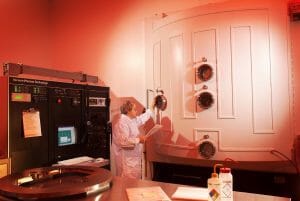
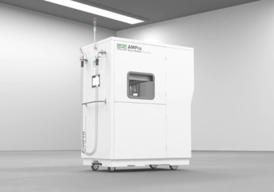
It is important to work with an optical manufacturing partner that has the expertise to translate a customer’s system level requirements into an optical tolerance for the mirror. As an example, the closer the aperture is to the edge of the optic the higher the cost, and there are several other considerations such as slope or surface roughness that need to be evaluated based on beam size and laser power. A good optics partner can walk with you through this process. (See Figures 3 & 4)
When looking at thin film coatings, the basic coating considerations include required spectral performance, critical wavebands, angle(s) of incidence, polarization, laser damage, durability, quantity of deliverable witness samples, and environmental factors. It goes without saying that it requires experience to marry all these considerations together.
Also, HEL applications typically require low loss coatings which can be stressful on an optic with CTE differences between the substrate and thin film coating. The reflected wavefront may be distorted after the coating is applied. Engaging your optics partner early in the design process will help mitigate the effects of coating stress.
It is also important to select an optics partner that has the capability to measure and compensate for that stress. Post-coat metrology may be problematic if there isn’t the metrology equipment available at the wavelengths needed. Without it, it may not be possible to know if the optic meets required performance criteria until it is integrated into the system, and this is the wrong time to find out that there is a problem.
Such issues are best mitigated during the design phase. Compensation techniques that can be used include finite element analysis (FEA), sample surrogate coating tests, polishing a bias into the cladding, stress compensation, coating on the backside.
- Figure 3. The coating room at ZYGO
- Figure 4. A Coating chamber at ZYGO
SUMMARY
When embarking on an HEL optics application, optical manufacturer partner selection is key to success. The chosen optical component expert should be viewed as a design partner not a job shop supplier, and must have extensive knowledge of the material properties and design parameters for the different flavours of SiC; no vested interest in promoting one specific type of material over another; attention to detail on cladding type and cladding requirements; metrology capabilities; the engineering resources to predict and mitigate common issues such as coating stress and print through; the programme management expertise for these types of applications; and also the thin film coating expertise, all under one roof.
Vertical integration is key.

