~ Application Specific Integrated Circuit (ASICs), System on Chip (SoC) or System in Package (SiP) — which do you choose? ~
According to Fictiv’s 2022 State of Manufacturing report, 90 per cent of manufacturers are using digital processes. Sitting at the heart of any digital strategy is a smart sensor that converts real-world variables into digitised data. But, as sensor technology grows in sophistication, how can we get all of this extra functionality into a miniature device for a reasonable cost? Here, Richard Mount, Director of Sales at ASIC design and supply company Swindon Silicon Systems, breaks down the ASIC, SoC and SiP integrated circuits (ICs) integral to intelligent sensors.
The majority of sensors convert a physical change into an electrical one. Understanding what this change means is a task for a higher-level control system. Once a manufacturer knows they want to integrate a smart sensor into their application, they’re bound to have some follow-up questions: what if the sensor can be made more sophisticated? How about conditioning the data and making the sensor response more linear? Calibrating the data to counter the effects of temperature, for example? Could the sensor filter unimportant events and only communicate changes that were relevant to the wider system?
Equipping a sensor with such functions doesn’t need to come at a cost that’s unfeasible for most manufacturers, and there are many forms of custom IC that can help achieve these ambitions.

ASICs
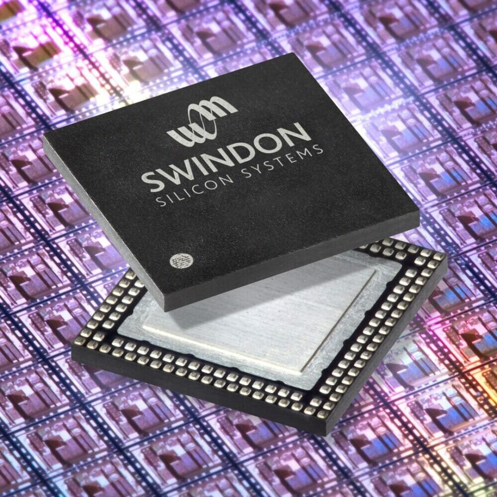
An ASIC is a custom chip that has been designed specifically for a customer’s individual application. This ensures that the ASIC is unique to any other offering on the market in terms of performance and differentiates the customer’s product from the competition.
ASICs are complex devices containing many functions. As well as including the processing, conditioning and communication functions required for sensor interfacing, designers working on today’s Industrial Internet of Things (IIoT) related products and systems find an ASIC will incorporate a number of cost and performance benefits.
While there is a short-term cost associated with ASIC development, the return on investment is high. By integrating functionality such as the analogue front end, signal processing and IoT connectivity into one system, the overall cost of the final product is much lower compared to its loaded PCB equivalent. Furthermore, because of its size and the fact that an ASIC replaces most of a PCB full of components, the user can expect a much higher efficiency and lower power consumption than they would receive from an off-the-shelf alternative.
Customers also choose the ASIC route to guarantee component supply for the lifetime of their product with no gaps in availability. Swindon, for instance, provides assurances that the device will be available until the customer end-of-lifes its product manufacture. This is in sharp contrast to a solution built using standard components, which are often at risk of obsolescence once the part no longer makes financial sense to the supplier.
SoC
When designing an ASIC, it often makes sense to integrate other parts of the circuit schematic onto the same silicon die. This is known as a System on Chip, which combines all the required analogue and digital functions of a typical IC, along with an embedded microprocessor. This means the SoC is a complete electronic substrate system that may contain analogue, digital, mixed-signal and radio frequency functions with the added advantage of a powerful processor at its core.
The main driver for this level of integration in a sensor is reduced size and lower bill of materials cost. To illustrate this, let’s look at proximity sensors as an example. Many of these sensors are no bigger than a finger, including sensor element and PCB sealed in a waterproof enclosure. Some 20 years ago, this level of integration would have been very challenging and out of reach for most companies, due to its cost and complexity. Now, alternatives such as SoC make fabricating these sensors far more accessible.
A SoC usually contains a variety of components that include, but are not limited to, software and programming, voltage regulators and power management circuits, analogue interfaces such as digital-to-analogue converters and vice-versa, a microprocessor and RAM and ROM memory. It comes with predesigned and pre-verified blocks, often called intellectual property (IP) blocks, obtained from either from the chip manufacturer themselves or from verified third parties and combined on a single chip.
Because a SoC includes both the hardware and software, it often uses less power, has better performance, requires less space and is more reliable than having multi-chip systems. Ultimately, a SoC product is designed to implement an entire embedded system on a single chip, thereby producing a system that is smaller, faster and can be easily integrated into its destined environment.

SiP
However, sometimes it is not possible to integrate all the system features into a single die and this is where a System in Package (SiP) comes to the fore. A SiP is typically an ASIC in bare die form that’s integrated with another IC, for example a microelectromechanical sensor (MEMS) or a communications die such as BLE, all in a single package. The ASIC provides the signal processing and sensor interface, while the MEMS acts as the sensing element and the BLE for a complex communications protocol.
Where a SoC refers to the encapsulation of CPUs, micro-controllers and other supporting hardware onto a single chip, a SiP is a further level of integration where multiple dies are integrated inside a single package. While a SoC contains all the required electronic elements, a SiP comprises individual chips accommodated in one package, each with a specific functionality. The result is a chip that provides considerable space savings and lower installation costs.
Dies containing the ICs can be stacked vertically on the substrate, connected by fine wires bonded to the package. Where a manufacturer would have needed multiple specialised IC devices to be assembled and connected on a PCB, that level of connectivity can be integrated into the package itself with a SiP.
One of the most notable advantages of using a SiP is its small size. Since a SiP uses IC manufacturing processes along with bare silicon die, it significantly reduces the size of the subsystem. This reduction in size allows designers to reduce the size of their PCB, supporting form factors that wouldn’t otherwise be possible. Furthermore, reduced assembly, PCB and materials costs will also make SiP more affordable, further increasing its accessibility.
For a manufacturer wanting to integrate more sophisticated, sensor-driven technology into their product, they may be pleased to know there are several options available at their fingertips. ASIC, SoC and SiP can all offer a multitude of performance gains that will help a product stand out from the competition. Knowing which option to choose, however, will require guidance from an expert in the design, test and supply of these integrated circuits.
To learn more about the ASIC, SiP and SoC options Swindon can deliver, visit the website to arrange a no-obligation first meeting.


